Traduction de l’étape 13
Étape 13


-
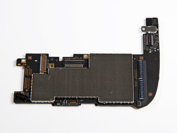
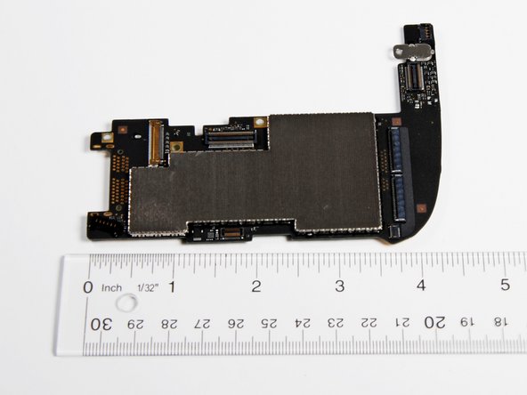
Top and bottom of logic board with the EMI shield on.
-
It looks like this board was made by AT&S. We haven't seen Apple's PCB manufacturers brand their boards before.
-
The logic board is about 4.5" wide, spanning about 60% of the iPad's width.
Vos contributions sont faites dans le cadre de la licence open source Creative Commons.